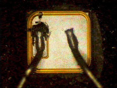
Photo 1 – External cracked package observed at Gate and Source lead of device #1.
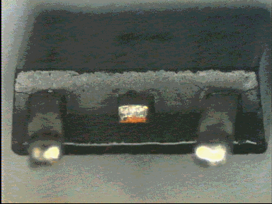
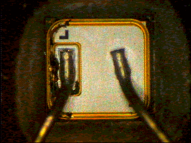
Photo 2 - External cracked package observed at Gate and Source lead of device #2.
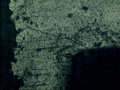
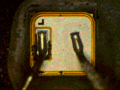
Photo 3 – External cracked package observed at Gate lead of device #3 (visible only at high power microscopic inspection).
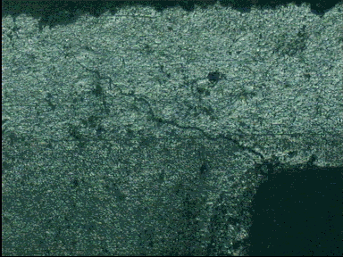
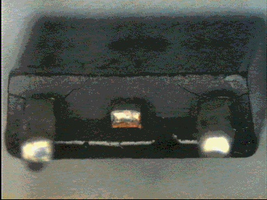
Photo 4 – External cracked package observed at Source lead of device #3 (visible only at high power microscopic inspection).