Photo #1: High power optical microscope image of unit #3 showing burnt/fused metal line at the failing pin’s I/O buffer at ME-2 suspected damaged due to EOS/ESD.


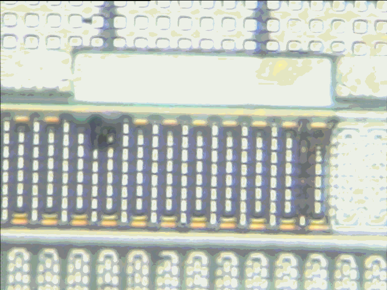
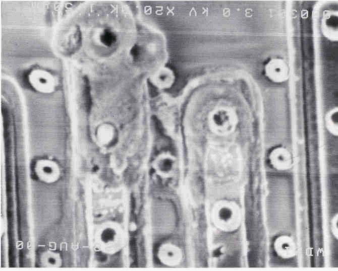
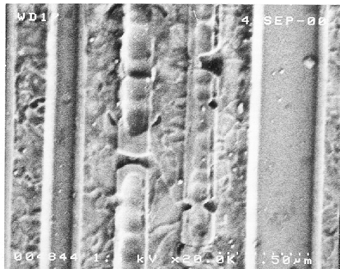
Photo #2: High power FESEM image of unit #3 showing burnt/fused metal line at the failing pin’s I/O buffer at ME-2 suspected damaged due to EOS/ESD.


Photo #3: Low power optical microscope image of unit #2 showing damage at the failing pin’s I/O buffer at silicon layer suspected damaged due to EOS/ESD.


Photo #4: Low power FESEM image of unit #2 showing damage at the failing pin’s I/O buffer at silicon layer suspected damaged due to EOS/ESD.

Photo #5: High power FESEM image of unit #2 showing damage at the failing pin’s I/O buffer at silicon layer suspected damaged due to EOS/ESD.