ESD CORNER
ESD Systems’ ESD Technical Newsletter
Issue 6, June 1999: Volume 2
Reference:
http://www.esdsystems.com/newsletters/v2issue6.htm
<<<=-=-=-=-=-=-=-=-=-=-=-=-=-=-=-=-=-=-=-=-=-=-=-=-=-=-=-=-=-=-=>>>
Sender :
ESD
Systems, 19 Brigham Street, # 9, Marlboro, MA 01752-3170
Phone
: 508-485-7390
E-mail :
editor@esdsystems.com
To be removed from this mailing list, send an e-mail
to ESD_Newletters@esdsystems.com
and put " UNSUBSCRIBE ESD_Newsletters" in the
subject.
This is a free monthly newsletter, which specializes on issues in static
control in the semiconductor/electronics workplace.
Need your own copy? Want to subscribe to this Newsletter? All you, or your
colleague(s), need to do is simply fill out the subscription form at
http://www.esdsystems.com/default.asp?PageNo=SENDEMAIL Let us know what
you think. Tell us what you would like to see in future issues. Want to
contribute articles or other related information to our Newsletter? Send your
comments to the
editor@esdsystems.com
<<<=-=-=-=-=-=-=-=-=-=-=-=-=-=-=-=-=-=-=-=-=-=-=-=-=-=-=-=-=-=-=>>>
IN
THIS ISSUE:
=-=-=-=-=-=-=-=-=-=-=-=
·
HOT TIP of the
MONTH (ESD Tape Applications)
·
21st
Annual EOS/ESD Symposium '99 (September 26-30)
·
ESD Q&A
CORNER (ESD Sensitive
Components)
·
PRODUCT
UPDATES (ESD Training Paddles)
·
Dr. ZAP (Components
and ESD Sensitivity)
HOT
TIP of the MONTH (ESD Tape
Applications)
=-=-=-=-=-=-=-=-=-=-=-=-=-=-=-=-=-=-=-=-=-=-=-=-=-=-=-=-=-=-=-=-=-=
Whenever tape is used in an ESD sensitive work area, only ESD tape should be used. The main reason is that standard tape, when unrolled, can generate tens of thousands of volts, exposing nearby ESD sensitive components to large electric fields. To minimize the risk from standard tape, we recommend using ESD tape depending on the application. Listed below are many applications for our ESD tape. Our ESD Clear (Acetate) Tape can be applied with the following applications: sealing bags, w/symbols for ESD awareness, general-purpose ESD tape applications, and Secure (bundle) IC tubes. The Red or Blue Acetate Tape can be used for identification or marking of product/paperwork/processes, attach paperwork to bags or product, and Secure (bundle) IC tubes. Conductive Shielding Tape can be used for applications requiring EMI shielding, in areas where the generation of static electricity is of high concern, and to Secure (bundle) IC tubes. ESD High Temperature Masking Tape can be use in applications masking PCB gold features for wave (hot air) soldering or soldering under 135 High Temperature ESD can be used for masking off PCB for wave soldering under 260oC in place of static generating kapton tapes. Aisle Marking Tape Can be used to mark off floors designating ESD Safe areas and can also be used as area signs.
1999 EOS/ESD Symposium
=-=-=-=-=-=-=-=-=-=-=-=-=-=-=-=-=
The 21st annual EOS/ESD Symposium is scheduled for the Wyndham Palace Resort in Orlando, FL, September 26-30, 1999.
The Symposium emphasizes the effects of electrical overstress (EOS), electrostatic discharge (ESD) and electrostatics on electronic and non-electronic devices, assemblies, systems, and processes.
Technical papers and authors corners will cover the latest research and technology. The technical program is supplemented by workshops and ESD training videos. The Symposium opens with two days of ESD seminars and tutorials.
Attendees will also have the opportunity to visit the exhibits of more than 100 companies who provide EOS and ESD control products and services.
Hundreds of attendees from throughout the world are expected to attend the annual event. The Symposium is sponsored by the ESD Association in cooperation with the IEEE. It is technically co-sponsored by the Electron Devices Society.
For more information on the Symposium, contact the 1999 EOS/ESD Symposium, c/o the ESD Association, 7900 Turin Rd., Building 3, Suite 2, Rome, NY 13440. Phone: 315-339-6937; Fax: 315-339-6793; e-mail: eosesd@aol.com Web Site: http://www.eosesd.org
ESD Q&A CORNER
=-=-=-=-=-=-=-=-=-=-=-=-=-=-=
The following questions and answers were selected from our FAQ WEB Page: http://www.esdsystems.com/question.html concerning Questions about ESD Sensitive Components and
Standards.
Q1: You have referenced standard EIA-625 on a couple of occasions. If my understanding is correct, this standard is for the minimum allowable voltage level in an ESD safe area. What exactly does this standard say and where could I get a copy of this standard. Thanks. - Anonymous, Nampa, ID Answers
A1: The ANSI/EIA-625-1994 standard is
labeled, “Requirements for Handling Electrostatic-Discharge-Sensitive (ESDS)
Devices.
SCOPE:
The Scope of this standard establishes the minimum requirements for Electrostatic
Discharge (ESD) control methods and materials used to protect electronic
devices that are susceptible to damage or degradation from electrostatic
discharge (ESD). The passage of a static charge through an
electrostatic-discharge-sensitive (ESDS) device can result in catastrophic
failure or performance degradation of the part.
ESD-sensitive devices are defined by appropriate documents (e.g., MIL-STD-883,
Test Method 3015, MIL-HDBK-263). ESDS devices with human body model
sensitivities of less than +/- 200 volts may need additional protective
measures beyond those specified in this standard.
OBTAIN A COPY:
As a service to our customers, we make this document available in our catalog
as item # 36050. You can also obtain a copy directly from Global Engineering
Documents, see details on out web site http://esdsystems.com/whitepapers/wp_standards.asp.
++++++++++++++++++++++++++++++++++++++++++
Q2: What is the best way to package and
handle components with Class 0 sensitivity? What type of materials should the
packaging consist of? Is “tape and reel” type packaging risky? What
specifications should the packaging comply with? - SuMei, Research In Motion,
Waterloo, Canada Answers
A2: The
best way to package and handle components with Class 0 sensitivity is to apply
all necessary control methods in order to keep the potential difference between
conductors below (100 V MM, 250 V HBM, 125 V CDM). This usually means your ESD
Control Program is more stringent and ionization is usually included at key
areas. If humans are handling the components, I suggest they wear grounded
wrist straps, static dissipative gloves and fully closed and grounded smocks.
That the work surfaces are static dissipative and grounded and all charge
generators are either removed or controlled with ionization. Testing of all
these parts is crucial too. Transportation of these parts should happen in
either a completely isolated and antistatic container or a shielded and fully
enclosed conductive container (Faraday cage) and these should only be opened at
a secure ESDS Class 1 area.
You should measure the fields (if any are generated) during the Tape and Reel
operation. If any significant fields are generated, then ionization should be
applied at these areas. The Tape and Reels should also be protected during
transportation as mentioned above.
There are several standards on ESD packaging. The ESDA has one on bags, ESD
S11.21-1994, ESD DS20.20-1998 section 6.2.4, EIA’s ANSI/EIA-625 section 8, and
a more detailed document just for “Packaging Material Standards for ESD
Sensitive Items” is ANSI/EIA-541.
++++++++++++++++++++++++++++++++++++++++++
Q3:
Where can I find the ESD Class rating for our purchased
electronic components? Do the Manufacturer catalogs have a spec that says that
this IC is a class I component? - Anonymous, Meridian, MS
Answers
A3:
The manufacturer
should be able to provide you with the various sensitivity ratings of their
devices. In lieu of this there is a data book publication VZAP-91P (ESD
Susceptibility Data) from the Reliability Analysis Center that has data on approximately
4000 devices including commercial part number, device description,
manufacturer, ESD Classification (per MIL-STD- 1686A and MIL-STD-883, Method
30157), data code, information regarding the source of the data, R/C values
used in the discharge circuit, failure voltage, pin combination, failure
criteria, and more.
PRODUCT UPDATES (
NEW!)
=-=-=-=-=-=-=-=-=-=-=-=-=-=-=-=-=-=-=-=-=-=
ESD Training Paddles easily generate high static
voltages
Ideal for Demonstrating Electrostatic Principles
· ESD Systems’ training paddles are an excellent tool for training employees and demonstrating electrostatic principles.
· Demonstrations include electric fields, field suppression, ionization, triboelectric generation, grounding, charge storage, capacitance, field induction, and electrical properties for both conductive and insulative materials.
· This kit includes one acrylic and one aluminum paddle for optimum charge generation, both with insulative handles.
· The 6” paddles are to be used in conjunction with a static field meter, ionization test kit, or charged plate analyzer.
Item #36080 is ideal for training, and we encourage you to give them a try! For more information and experiments to perform with the paddles, request Tech Brief PS-2079.
Dr.
ZAP
=-=-=-=-=-=
Topic:
Information gleaned from white paper on Components
and ESD Sensitivity: http://www.esdsystems.com/whitepapers/wp_devicesandstatic.asp
Components and ESD
Sensitivity
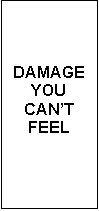
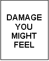
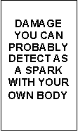
Devices have various levels of sensitivity. A
chart from MIL-STD-1686C and reprinted in the ESD Awareness Guide from ESD
Systems semiconductor/electronics will give you a partial list of various
devices and their sensitivity levels.
DEVICE SENSITIVITY TO
ELECTROSTATIC DISCHARGE
Human Body Model (HBM)
ESD Class 0-1C: 0 to 1999 volts
The following devices or microcircuits were identified by test
data as class 1:
 Microwave and high frequency devices
(Schottky barrier diodes, probe contact diodes, other detector diodes)
Discrete MOSFET devices
SAW
JFETS
CCDs
Precision voltage regulator diodes
OP AMP
Thin film resistors
Integrated circuits
Hybrids utilizing class 1 parts
VHSIC
SCRs
ESD Class 2: 2,000 to 3,999 volts
 Devices or microcircuits when identified by appendix A test
data as class 2:
Devices or microcircuits when identified by appendix A test
data as class 2:
Discrete MOSFET devices
JFETs
ICs
VHSIC
Precision resistor networks (type RZ)
Hybrids utilizing class 2 parts
Low power bipolar transistors
ESD Class 3A-3B: 4,000 to over 8,000 volts
 Devices or microcircuits when identified by appendix A test
data as class 3:
Devices or microcircuits when identified by appendix A test
data as class 3:
Discrete MOSFET devices
JFETs
OP AMPS
ICs
VHSIC
All other microcircuits not included in class 1 or class 2
Small signal diodes
General-purpose silicon rectifiers
Opto-electronic devices (LEDs, photo transformers, opto couplers)
Resistor chips
Piezo electric crystals
Hybrids using Class 3 parts
ESDS classifications are from U.S. Department of Defense,
MIL-STD-1686C, 25 October 1995.
Refer to this document for Machine Model (MM) and Charged Device Model (CDM)
ESDS classifications.
A revised level of sensitivity for ESD sensitive components is shown in the ESD
Association document ESD-STM5.1-1998 (Electrostatic Discharge (ESD) Sensitivity
Testing) on page 2. It is
reprinted here because it is important information when you determine the level
of your ESD program.
HMB ESDS Component Classification
|
Class |
Voltage
Range |
|
0 |
<250 |
|
1A |
250 to <500 |
|
1B |
500 to <1000 |
|
1C |
1000 to < 2000 |
|
2 |
2000 to < 4000 |
|
3A |
4000 to < 8000 |
|
3B |
> or + 8000 |
Normal activity within a production facility regarding triboelectric charging levels of operators and objects given in voltages and dependent on relative humidity.
|
Table 1 TYPICAL ELECTROSTATIC VOLTAGES |
|||
|
EVENT |
RELATIVE HUMIDITY |
||
|
10% |
40% |
55% |
|
|
Walking
across carpet |
35,000 |
15,000 |
7,500 |
|
Walking
across vinyl floor |
12,000 |
5,000 |
3,000 |
|
Motions
of bench worker |
6,000 |
800 |
400 |
|
Remove
DIPs from plastic tubes |
2,000 |
700 |
400 |
|
Remove
DIPs from vinyl trays |
11,500 |
4,000 |
2,000 |
|
Remove
DIPs from Styrofoam |
14,500 |
5,000 |
3,500 |
|
Remove
bubble pack from PCBs |
26,000 |
20,000 |
7,000 |
|
Pack
PCBs in foam-lined box |
21,000 |
11,000 |
5,500 |
Difference in component sensitivity between through-hole and surface mount devices is dependent on the architecture and technology packaged. Typically, surface mount devices have much smaller architecture making them even more susceptible to ESD than through-hole packaged devices.
Technology Trends |
|||||
|
|
1995 |
1998 |
2001 |
2004 |
2007 |
|
Feature size (mm) |
0.35 |
0.25 |
0.18 |
0.12 |
0.10 |
|
Voltage (V) |
3.5 |
2 - 3.5 |
1.50 – 1.9 |
1.0 – 1.5 |
1.0 |
Source: Terry Welsher, Bell
Labs, Lucent Technologies, 12/2/97 NE Chapter ESD Association general meeting
For IC packaging, the I/O count has climbed from 600 to 1,000 to well over this now.
Ball Grid Array Chips are replacing through hole pin chip technology.
A typical electronics company looses 5% of revenue from all causes of product failure. Even with all ESD programs in place.
Cost avoidance is the biggest issue.
21% of failure analysis is due to electronics and most are ESD.
ROI
The ROI on an ESD control program is 95:1. For every one-dollar invested in ESD control, ninety-five dollars comes back as money saved.
<<<=-=-=-=-=-=-=-=-=-=-=-=-=-=-=-=-=-=-=-=-=-=-=-=--=>>>
This is a free monthly newsletter, which specializes on
issues in static control in the
semiconductor/electronics
workplace.
Need your own copy? Want to subscribe to this Newsletter? All you or your
colleague(s) need to do is simply fill out the subscription form at http://www.esdsystems.com/forms/esdmail.asp
This
Newsletter is never sent unsolicited. To unsubscribe from this mailing, send an
e-mail to ESD_Newletters@esdsystems.com
and put " UNSUBSCRIBE ESD_Newsletters"
in the subject.
Let us know what you think. Tell us what you would like to see in future
issues. Want to contribute articles or other related information to our
Newsletter? Send your comments to the editor@esdsystems.com
Copyright © Desco Industries,
Inc. 1999
END V2I6